| Decimal (base 10) | Binary (base 2) | Octal (base 8) | Hexadecimal (base 16) |
| 00 01 02 03 04 05 06 07 08 09 10 11 12 13 14 15 | 0000 0001 0010 0011 0100 0101 0110 0111 1000 1001 1010 1011 1100 1101 1110 1111 | 00 01 02 03 04 05 06 07 10 11 12 13 14 15 16 17 | 0 1 2 3 4 5 6 7 8 9 A B C D E F |
Wednesday, September 22, 2010
Numbers with Different Base (Number System)
Complements
Complements are used in digital computers for simplifying the subtraction operation and for logical manipulations. There are two types of complements for each base-r system: (1) the r’s complement and (2) the (r-1)’s complement. When the value of the base is substituted, the two types receive the names 2’s and 1’s complement for binary numbers, or 10’s and 9’s complement for decimal numbers:
The r’s Complement:
Given a positive number N in base r with an integer part of n digits, the r’s complement of N is defined as rn-N for N≠0 and 0 for N=0. The following numerical example will help clarify the definition.
The 10’s complement of (52520)10 is 105 – 52520 = 47480.
The number of digits in the number is n = 5.
The 10’s complement of (0.3267)10 is 1 – 0.3267 = 0.6733.
No integer part, so 10n = 100 = 1.
The 10’s complement of (25.639)10 is 102 – 25.639 = 74.361.
The 2’s complement of (101100)2 is (26)10 – (101100)2 = (1000000 – 101100)2 = 010100.
The 2’s complement of (0.0110)2 is (1 – 0.0110)2 = 0.1010.
The (r – 1)’s Complement:
Given a positive number N in base r with an integer part of n digits and a fraction part of m digits, the (r – 1)’s complement of N is defined as rn – r-m – N. Some numerical examples follow:
The 9’s complement of (52520)10 is (105 – 1 – 52520) = 99999 – 52520 = 47479.
No fraction part, so 10-m = 100 = 1.
The 9’s complement of (0.3267)10 is (1 – 10-4 – 0.3267) = 0.9999 – 0.3267 = 0.6732.
No integer part, so 10n = 100 = 1.
The 9’s complement of (25.639)10 is (102 – 10-3 – 25.639) = 99.999 – 25.639 = 74.360.
The 1’s complement of (101100)2 is (26 – 1)10 – (101100)2 = (111111 – 101100)2 = 010011.
The 1’s complement of (0.0110)2 is (1 – 2-4)10 – (0.0110)2 = (0.1111 – 0.0110)2 = 0.1001.
Postulates and Theorems of Boolean Algebra
| Postulate 2 Postulate 5 Theorem 1 Theorem 2 Theorem 3, involution Postulate 3, commutative Theorem 4, associative Postulate 4, distributive Theorem 5, DeMorgan Theorem 6, absorption | x + 0 = x x + x’ = 1 x + x = x x + 1 = 1 (x’)’ = x x + y = y + x x + (y + z) = (x + y) + z x (y + z) = xy + xz (x + y)’ = x’y’ x + xy = x | x . 1 = x x . x’ = 0 x . x = x x . 0 = 0
xy =yx x(yz) = (xy)z x + yz = (x + y)(x + z) (xy)’ = x’ + y’ x(x + y) = x |
Minterms and Maxterms for three Binary Variables
Minterms | Maxterms | |||
| x y z | Term | Designation | Term | Designation |
| 0 0 0 0 0 1 0 1 0 0 1 1 1 0 0 1 0 1 1 1 0 1 1 1 | x’ y’ z’ x’ y’ z x’ y z’ x’ y z x y’ z’ x y’ z x y z’ x y z | m0 m1 m2 m3 m4 m5 m6 m7 | x + y + z x + y + z’ x + y’+ z x + y’+ z’ x’+ y + z x’+ y + z’ x’+ y’+ z x’+ y’+ z’ | M0 M1 M2 M3 M4 M5 M6 M7 |
Karnaugh Map (K Map)
The diagram below illustrates the correspondence between the Karnaugh map and the truth table for the general case of a two variable problem.
The values inside the squares are copied from the output column of the truth table, therefore there is one square in the map for every row in the truth table. Around the edge of the Karnaugh map are the values of the two input variable. A is along the top and B is down the left hand side. The diagram below explains this:
The values around the edge of the map can be thought of as coordinates. So as an example, the square on the top right hand corner of the map in the above diagram has coordinates A=1 and B=0. This square corresponds to the row in the truth table where A=1 and B=0 and F=1. Note that the value in the F column represents a particular function to which the Karnaugh map corresponds.


Universal Gate
Universal Gates:
A universal gate is a gate which can implement any Boolean function without need to use any other gate type.
The NAND and NOR gates are universal gates.
In practice, this is advantageous since NAND and NOR gates are economical and easier to fabricate and are the basic gates used in all IC digital logic families.
In fact, an AND gate is typically implemented as a NAND gate followed by an inverter not the other way around.
Likewise, an OR gate is typically implemented as a NOR gate followed by an inverter not the other way around.
NAND Gate is a Universal Gate:
To prove that any Boolean function can be implemented using only NAND gates, we will show that the AND, OR, and NOT operations can be performed using only these gates.

NOR Gate is a Universal Gate:
To prove that any Boolean function can be implemented using only NOR gates, we will show that the AND, OR, and NOT operations can be performed using only these gates.

Adder
Half adder:
A half adder is a logical circuit that performs an addition operation on two one-bit binary numbers often written as A and B. The half adder output is a sum of the two inputs usually represented with the signals Cout and S where sum=2*Cout+S. Following is the logic table for a half adder:
| Inputs | Outputs | ||
| A | B | C | S |
| 0 | 0 | 0 | 0 |
| 0 | 1 | 0 | 1 |
| 1 | 0 | 0 | 1 |
| 1 | 1 | 1 | 0 |

Example half adder circuit diagram
As an example, a Half Adder can be built with an XOR gate and an AND gate.
___________A ------| |
| Half |----- S=A(+)B
| Adder |
| |----- C=A.B
B ------|___________| Full adder:
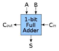
Schematic symbol for a 1-bit full adder with Cin and Cout drawn on sides of block to emphasize their use in a multi-bit adder.
A full adder is a logical circuit that performs an addition operation on three one-bit binary numbers often written as A, B, and Cin. The full adder produces a two-bit output sum typically represented with the signals Cout and S where sum=2*Cout+S. The full adder's truth table is:
| Inputs | Outputs | |||
| A | B | Ci | Co | S |
| 0 | 0 | 0 | 0 | 0 |
| 1 | 0 | 0 | 0 | 1 |
| 0 | 1 | 0 | 0 | 1 |
| 1 | 1 | 0 | 1 | 0 |
| 0 | 0 | 1 | 0 | 1 |
| 1 | 0 | 1 | 1 | 0 |
| 0 | 1 | 1 | 1 | 0 |
| 1 | 1 | 1 | 1 | 1 |
A full adder can be implemented in many different ways such as with a custom transistor-level circuit or composed of other gates. One example implementation is with S=(A(+)B)(+)Cin and Cout=(A.B)+(Cin.(A(+)B)).

Example full adder circuit diagram
Inputs: {A, B, Cin} → Outputs: {S, Cout}
Example full adder circuit diagram using only NAND and XOR gates
Inputs: {A, B, Cin} → Outputs: {S, Cout}
In this implementation, the final OR gate before the carry-out output may be replaced by an XOR gate without altering the resulting logic. Using only two types of gates is convenient if the circuit is being implemented using simple IC chips which contain only one gate type per chip.
A full adder can be constructed from two half adders by connecting A and B to the input of one half adder, connecting the sum from that to an input to the second adder, connecting Ci to the other input and OR the two carry outputs. Equivalently, S could be made the three-bit XOR of A, B, and Ci, and Co could be made the three-bit majority function of A, B, and Ci.
Tuesday, September 21, 2010
Digital IC Terminology
Current and voltage Parameters:

· VIH(min)-High Level Input Voltage: The minimum voltage level required for a logical 1 at an input. Any voltage below this level will not be accepted as a HIGH by the logic circuit.
· VIL(max)-Low Level Input Voltage: The maximum voltage level required for a logical 0 at an input. Any voltage above this level will not be accepted as a LOW by the logic circuit.
· VOH(min)-High Level Output Voltage: The minimum voltage level at a logic circuit output in the logical 1 state under defined load conditions.
· VOL(max)-Low Level Output Voltage: The maximum voltage level at a logic circuit output in the logical 0 state under defined load conditions.
· IIH(min)-High Level Input Current: The current that flows into an input when a specified high level voltage is applied to that input.
· IIL(max)-Low Level Input Current: The current that flows into an input when a specified low level voltage is applied to that input.
· IOH(min)-High Level Output Current: The current that flows from an output in the logical 1 state under specified load conditions.
· IOL(max)-Low Level Output Current: The current that flows from an output in the logical 0 state under specified load conditions.

The high state noise margin VNH is defined as
VNH=VIH(min)-VOH(min)
The low state noise margin VNL is defined as
VNL=VIL(max)-VOL(max)
Carry Propagation
The addition of two binary numbers in parallel implies that all the bits of the angend and addend are available for computation at the same time.
As in any combinational ckt, the signal must propagate through the gates before the correct output sum is available in the output terminals.
A binary parallel adder is a digital function that produces the arithmetic sum of two binary numbers in parallel. It consists of full adders connected in cascade, with the output carry from one full adder connected to the input carry of the next full adder.

Figure shows the interconnection of 4 full adder (FA) ckts to provide a 4 - bit binary parallel adder. The augend bits of A and the addend bits of B are designated by subscript numbers from right to left, with subscript 1 denoting the low order bit. The carries are connected in a chain through the full adders. The input carry to the adder is C1 and the output carry is C5. The S outputs generate the required sum bits. When the 4 bit full adder ckt is enclosed within an IC package, it has four terminals for the augend bits, four terminals for the addend bits, four terminals for the sum bits, and two terminals for the input and output carries.
Binary Coded Decimal (BCD) Adder
Consider the arithmetic addition of two decimal digits in BCD together with a possible carry from a previous stage.
Each input digit does not exceed 9, the output sum cannot be greater than 9+9+1=19.
This adder will from the sum in binary and produce a result which may range from 0 to 19.
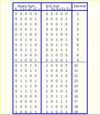
We found the derivation of a BCD adder, when the binary sum is equal to or less than 1001, the corresponding BCD number is identical.
When the binary sum is greater then 1001, the addition of binary 6(0110) to the binary sum converts it to the correct BCD representation and also produces an output carry as required.
An output carry can be expressed by the Boolean function: C=K+Z8Z4+Z8Z2: When C=1, it is necessary to add 0110 to the binary sum and provide an output carry for the next stage.

A decimal parallel adder that adds n decimal digits needs n BCD adder stages. The output carry one stage must be connected to the input carry of the next higher order stage.
Magnitude Comparator
A magnitude comparator is a combinational ckt that compares two numbers, A and B, and determines their relative magnitudes.
The outcomes of the comparison is specified by three binary variables that indicate whether A>B, A=B or A
Consider two numbers A and B, with four digits each A=A3A2A1A0 and B=B3B2B1B0
The equivalence function: xi=AiBi+A’iB’i as i=0,1,2,3,….
If (A=B)=x3x2x1x0
(A>B)=A3B’3+x3A2B’2+x3x2A1B’1+x3x2x1A0B’0
(A

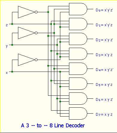
Decoder
A decoder is a combinational ckt that converts binary information from n input lines to a maximum of 2n unique output lines.
If the n-bit decoded information has unused or don’t care combinations, the decoder output will have less than 2n outputs.
Encoder
An encoder is a digital function that produces a reverse operation from that of a decoder. An encoder has 2n(or less) input lines and n output lines. The output lines generate the binary code for the 2n input variables.
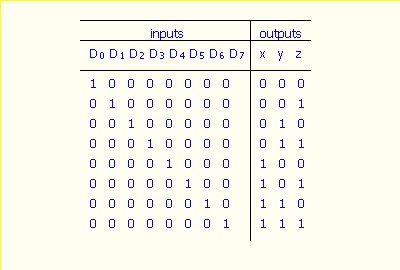
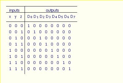
We found from truth table x=D4+D5+D6+D7; y=D2+D3+D6+D7; z=D1+D3+D5+D7

D0 is not connected to any OR gate; the binary output must be all 0’s in this case.
The ckt has 8 inputs and could have 28=256 possible input combinations. Only 8 of these combinations have any meaning. The other inputs combinations are don’t care conditions.
Multiplexer
Multiplexing means transmitting a large number of information units over a smaller number of channels or lines. A digital multiplexer is a combinational ckt that selects binary information from one of many input lines and directs it to a single output line. The selection of a particular input line is controlled by a set of a selection lines. There are 2n input lines and n selection lines whose bit combinations determine which input is selected.

A in decoders, multiplexer ICs may have an enable input to control the operation of the unit. When the enable input is in a given binary state, the outputs are disabled, and when it is in the other state (the enable state), the ckt functions as a normal multiplexer. The enable input can be used to expand two or more multiplexer ICs to a digital multiplexer with a larger number of inputs.
Demultiplxer
· A decoder with an enable input can function as a demultiplexer. A demultiplexer is a ckt that receives information on a single line and transmits this information on one of 2n possible output lines.
· A decoder with an enable input is referred to as a demultiplexer. It is the enable input that makes the ckt a demultiplexer.


· If E is 0 then one demultiplexer is enabled and the other is disabled and for E is 1 then vice-versa.
Monday, September 20, 2010
Read Only Memory (ROM)
· A ROM is a device that includes both the decoder and the OR gates with in a single IC package.
· Block diagram shows, n inputs lines, each bit is called an address and m output lines, each bit is called a word.

· The ROM is very often used to implement a complex combinational ckt in one IC package.
· A ROM is essentially a memory device in which a fixed set of binary information is stored.
· ROMs have many important applications in the design of digital computer systems.
Thursday, September 16, 2010
Programmable Logic Array (PLA)
· PLA is similar to a ROM in concept, but the PLA does not provide full decoding of the variables and does not generate all the minterms as in the ROM. In PLA, the decoder is replaced by a group of AND gates.
· PLA consists of n inputs, m (OR gate) outputs, K (AND gate) product terms and m sum terms.
· The PAL is the opposite of the ROM, having a programmable set of ANDs combined with fixed ORs.
· Compared to a ROM and a PAL, a PLA is the most flexible having a programmable set of ANDs combined with a programmable set of ORs.
Advantages:
o A PLA can have large N and M permitting implementation of equations that are impractical for a ROM (because of the number of inputs, N, required
o A PLA has all of its product terms connectable to all outputs, overcoming the problem of the limited inputs to the PAL Ors
o Some PLAs have outputs that can be complemented, adding POS functions
Disadvantages:
o Often, the product term count limits the application of a PLA.
o Two-level multiple-output optimization is required to reduce the number of product terms in an implementation, helping to fit it into a PLA.
o Multi-level circuit capability available in PAL not available in PLA. PLA requires external connections to do multi-level circuits.

3-input, 3-output PLA with 4 product terms.
The IC Digital Logic Families
The IC Digital Logic Families:
· RTL-Resistor-Transistor Logic.
· DTL-Diode-Transistor Logic.
· I2L-Integrated-Injection Logic.
· TTL-Transistor-Transistor Logic.
· ECL-Emitter-Coupled Logic.
· MOS-Metal-Oxide Semi-conductor.
· CMOS-Complementary Metal-Oxide Semi-conductor.
Advantage of CMOS:
· Ckt is must simpler.
· Easy to fabricate.
· Faster.
· Power consumption is low.
· Comparatively cheeper.
Disadvantage of CMOS is the logic is always invert.

Subscribe to:
Posts (Atom)